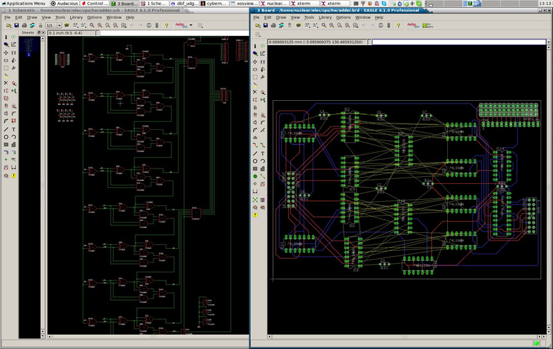
Progress shot of the schematic and PCB design.

Progress shot of the schematic and PCB design.
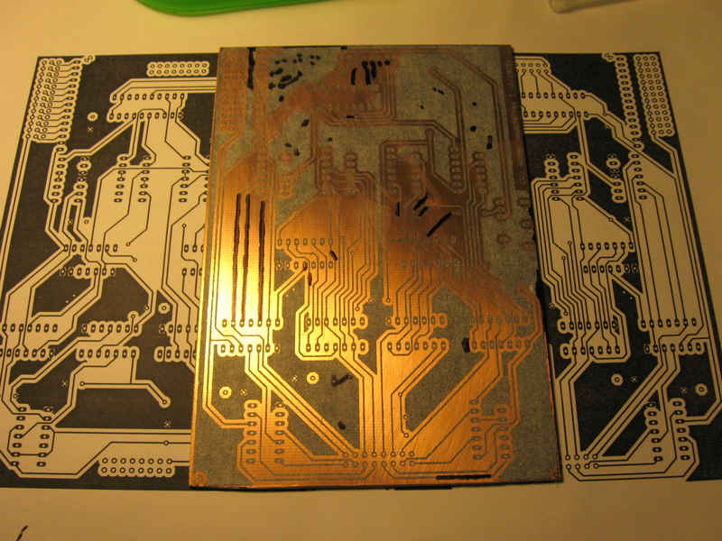
The PCB toner transfer was mostly successful. The result is salvageable
by passing over broken and hair-thin traces with a sharpie. Also painted over
holes in the ground plane which is definitely not required, but I thought they
might be confusing while drilling later (and ugly).
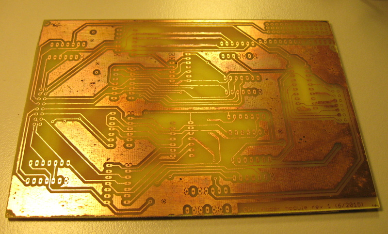
After etching, the PCB looks usable. Sharpie fixups definitely worked; might need
some solder touchups here and there to fix broken traces.
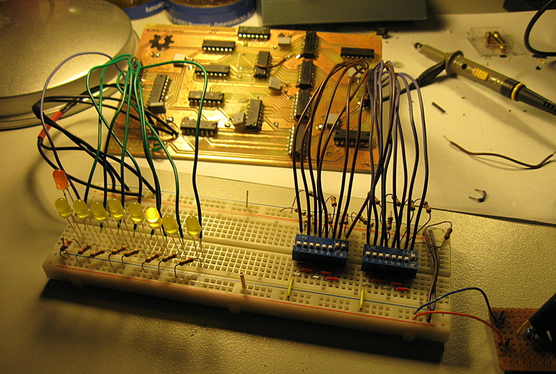
Running a few manual tests with DIP-switches and LEDs, after completing the
assembly of the adder board.